


Veuillez noter que pour la date listée ci-dessous, les services de production et d’expédition ne sont pas considérés comme jour ouvré:
- 01.05.2024
- 09.05.2024 et 10.05.2024
- 20.05.2024
- 30.05.2024 et 31.05.2024
Step 1
Step 1
After receiving your order including data, our goal is to begin production of your printed circuit boards within 24 hours. Here the 16 man and woman strong technology team support in the Würth Elektronik branch Mysore in India. Due to the WE internal cooperation, your data will always remain in our house, but can be processed almost around the clock for our systems. In cooperation with WEdirekt Engineering in Germany, the course is set for successful production.
Standard technologies are pooled - after clearing up all clarifications - to optimize production utilization. On the other hand, "More Technology" orders are produced individually in order to achieve the best possible delivery times. Finally, the NC programs of our production panel are created before the collected data is released for production.
Step 2
Step 2
After completion of the data preparation, our production planning will ensure a smooth process and punctual completion of your orders. Key to the success is the optimization of our production. Not an easy task, considering that every day about 550 production panels move through our production and are processed in a two-shift system.
As soon as your order is released for our production, it can start up without long delays. The basis for this is our material supply. The basic materials are always available in time. Now everything is prepared so that your data and our material can come together.
Step 3
Step 3
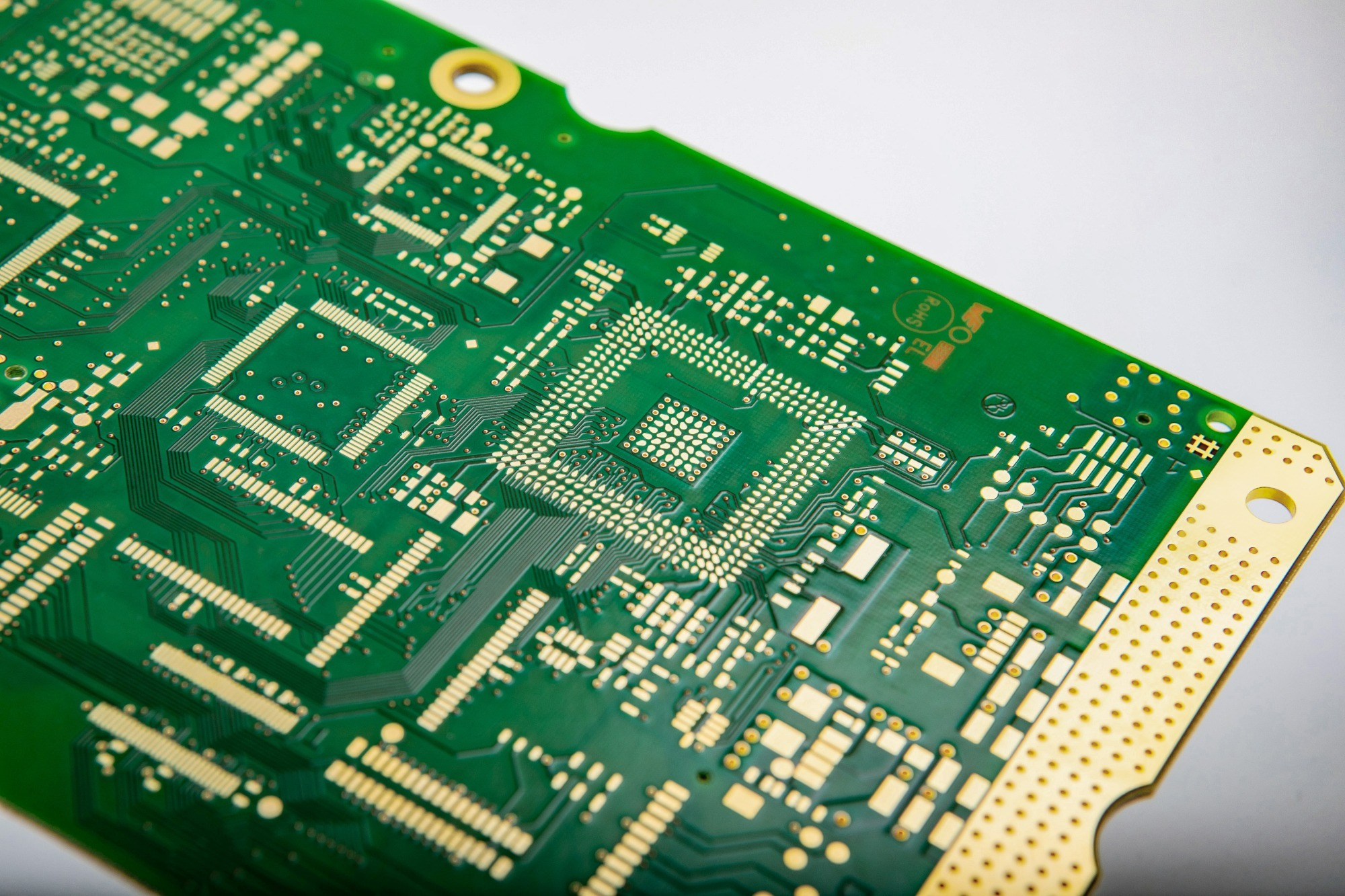
The layout you have designed will be worked out for us from fully coated copper panels / foils. The first steps to the finished circuit pattern are prepared by our photo printing department. After thorough pre-cleaning and roughening of the copper surface, a photoresist is laminated under dimmed light.
Your layout will then be applied on the prepared data by direct exposure. Depending on the manufacturing process, the required printed conductors and pads can be protected from etching baths or released for the copper structure.
After the inner layers of the PCB have been completed in this way, the order for pressing, before the two outer layers ultimately get their conductor pattern.
Step 4
Step 4
After successful production of the inner layers of your PCBs, the layer structures are assembled with different prepreg combinations (FR4 material). The laying and allocation of the materials are still done manually. Under vacuum and prescribed heat history, these are pressed before the individual layers are connected again through via holes.
Depending on the number of layers and the complexity of the structure, this pressing process can be repeated several times. Precise and clean working are the basic prerequisites for avoiding inclusions between the layers or even a misalignment of the layers.
Before the production panels are handed over to the next operation, there is still a removal of excess material and a cleaning process.
Step 5
Step 5
In order to connect the various layers of your layout with each other, the PCBs initially go to the mechanical process, drilling.
At the beginning, locating and registration holes are introduced into our production panel so that human error can be minimized as far as possible. This is done fully automatically and by means of X-ray of the PCB inner layers.
The panels are then fed into the individual drilling machines via a loading system. Each of the buffers can hold up to 20 drill packages and they are processed according to priority. Before the intended vias and component holes are created, the drilling pattern is aligned again using the previously introduced registration features.
Now the tools of between 0.2mm and 6.0mm can start processing the material at rotational speeds of up to 300,000 rpm. Before the PCBs make their next departmental change, all panels are rechecked for burr or offset. This maintains the quality level and detects any potential errors early. Now the PCBs are prepared and ready for through hole plating.
Step 6
Step 6
After the processed drill packages have been separated again, the production panels are ready for through-connection. First a cleaning process is done to remove any burrs. Then enough copper is applied during the first pass to metallize the drill sleeves and also to electrically connect the individual layers. In a second pass, the pattern of the outer layers is brought to the desired end copper thickness. The printed circuit board is already functional in this state.
In the next production step, the solder resist is applied by screen printing. The photosensitive resist, which is initially applied fully on all sides, is exposed and developed regarding the desired pads. The curing of the resist under heat ensures durability and resistance.
The created clearances are then covered in a chemical process with a solderable surface. Our standard is ENIG with a layer thickness of 4-7 μm nickel and 0.05-0.1 μm gold. This refinement serves for improved solderability and durability. Depending on the customer's request, a service print can additionally be applied to the boards before they are passed on to mechanical finishing.
Step 7
Step 7
Sobald unsere Produktionspanel nach den chemischen Prozessen wieder in die mechanische Bearbeitung gegeben werden, befinden sich Ihre Leiterplatten kurz vor der Fertigstellung.
Zuerst werden eventuell benötigte Kerbritzungen eingebracht und Liefernutzenaustrennungen vorgesehen. Anschließend wird die Kontur ausgefräst wodurch die Aufträge wiederum kundenspezifisch separiert werden. Aus einem Produktionspanel werden so bis zu sechs Kundenaufträge.
Abhängig vom Fräsdurchmesser, der meist durch die Leiterplatten-Kontur definiert wird, können die Aufträge im einzelnen Produktionspanel oder im Paket bearbeitet werden um eine möglichst hohe Maschinenauslastung zu erhalten. Anschließend werden die PCBs noch einer Reinigung unterzogen um etwaige Grate und den Frässtaub zu entfernen. So können die Leiterplatten dann in der Endkontrolle korrekt bewertet werden.
Step 8
Step 8
After the PCBs have been separated according to customer specifications in the previous step and have received a final cleaning, we check each piece again against the corresponding production documents. In addition to an optical sighting to avoid scratches and superficial damage, the dimensional accuracy of the LP is also tested. For this purpose, we use the usual measuring means. For example an enlargement camera, calipers, magnifying glass or test probes. If you have decided to request a CoC (Certificate of Conformity) with your order, this will also be created here.
Afterward, the printed circuit boards are welded and labeled in order to exclude further sources of damage and to ensure a clear assignability. Our shipping department then collects the products of your order and packs them in the "red" book box, where you can easily recognize our shipments. If this is already available before the confirmed shipping date, we will send your package immediately and do not keep it in stock. Of course, we are still available to you after receiving your order and are happy to help you with any questions.